Week 8 – Circuit Manufacturing
The Idea of this week is to manufacture a USB to UPDI convert. For this a PCB board needs to be manufactured with a milling machine. Furthermore all needed components need to be solder to the board and check for functionality. This week assignment is based on board design and data provided from fabacadamy:https://fabacademy.org/2022/labs/kamplintfort/resorces/ft230x-updi.html
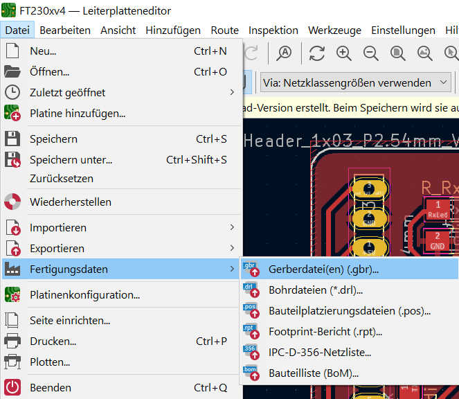
Firstly a PCB board needs to be constructed. Download the file provided from the link above. This will provide a Kicad File, that descriptes the layout diagram and the circuit diagram. Open the .kicad_pcb for an overview of the board. For this step the layout diagram is only important to create the PCB. If the file is imported right, a list of layers will appear on the left representing board connection layout, board cutout layout etc. This file can be directly exported for the CNC Machine program by selecting files > manufacture > gerberdatei. A setup window will appear, where layers for manufacturing need to be selected. Only Select the F.Cu and Edge.cut layers, to mill only the top of the board and to cutout it out. Select a folder where the new files should be saved and check if the units a correct.
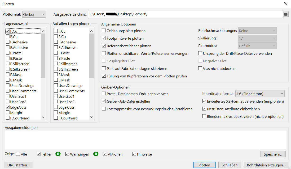
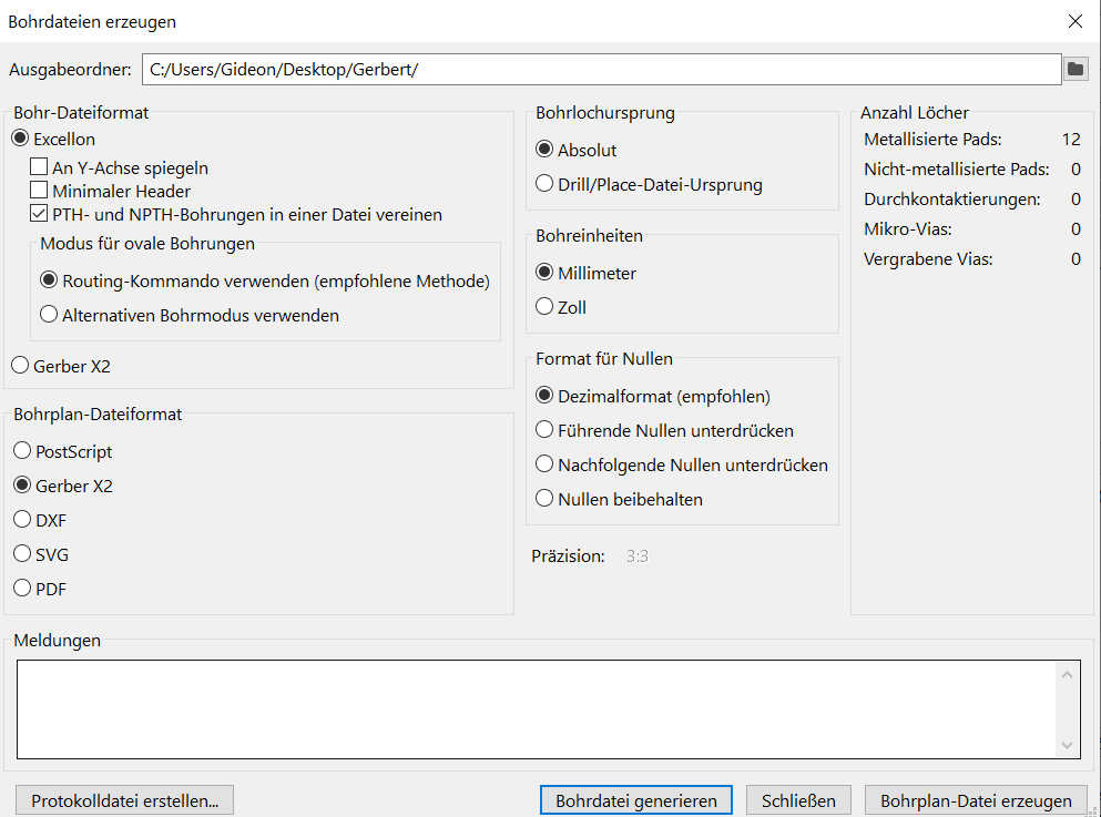
Now a drill file needs to be created from this setting by selecting generate drilling file. In this window set drill origin to absolute and set the units to millimeter. Tick the box at gerber X2 to define the filetype. Now click to generate a drill plan and than press generate drill file.This window can now be closed and go back to the setup window. Select plot, this will generate 3 more files, the job file, F_Cu.gbr and Edge_Cuts.gbr. These files should be enough to manufacture the PCB board.
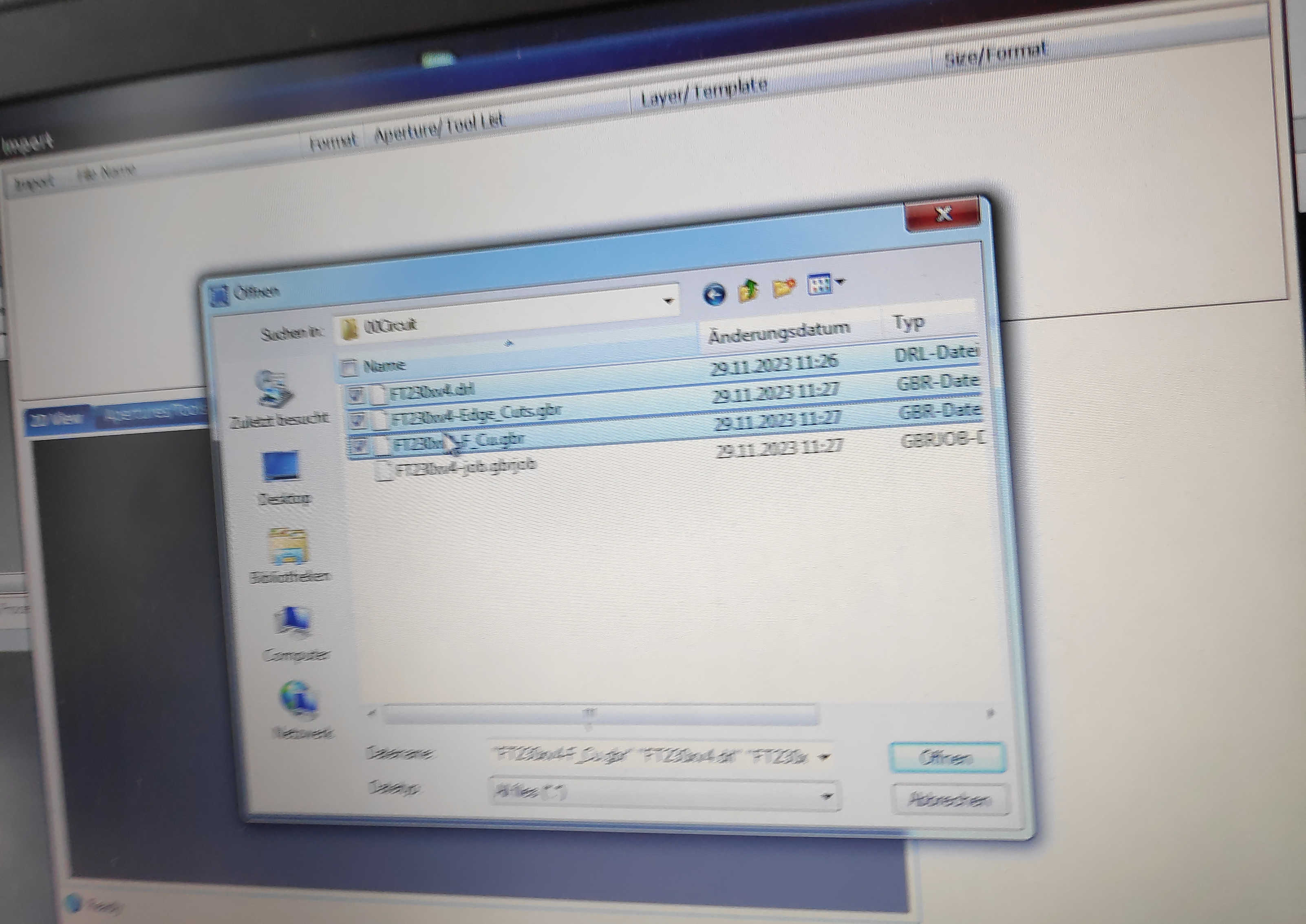
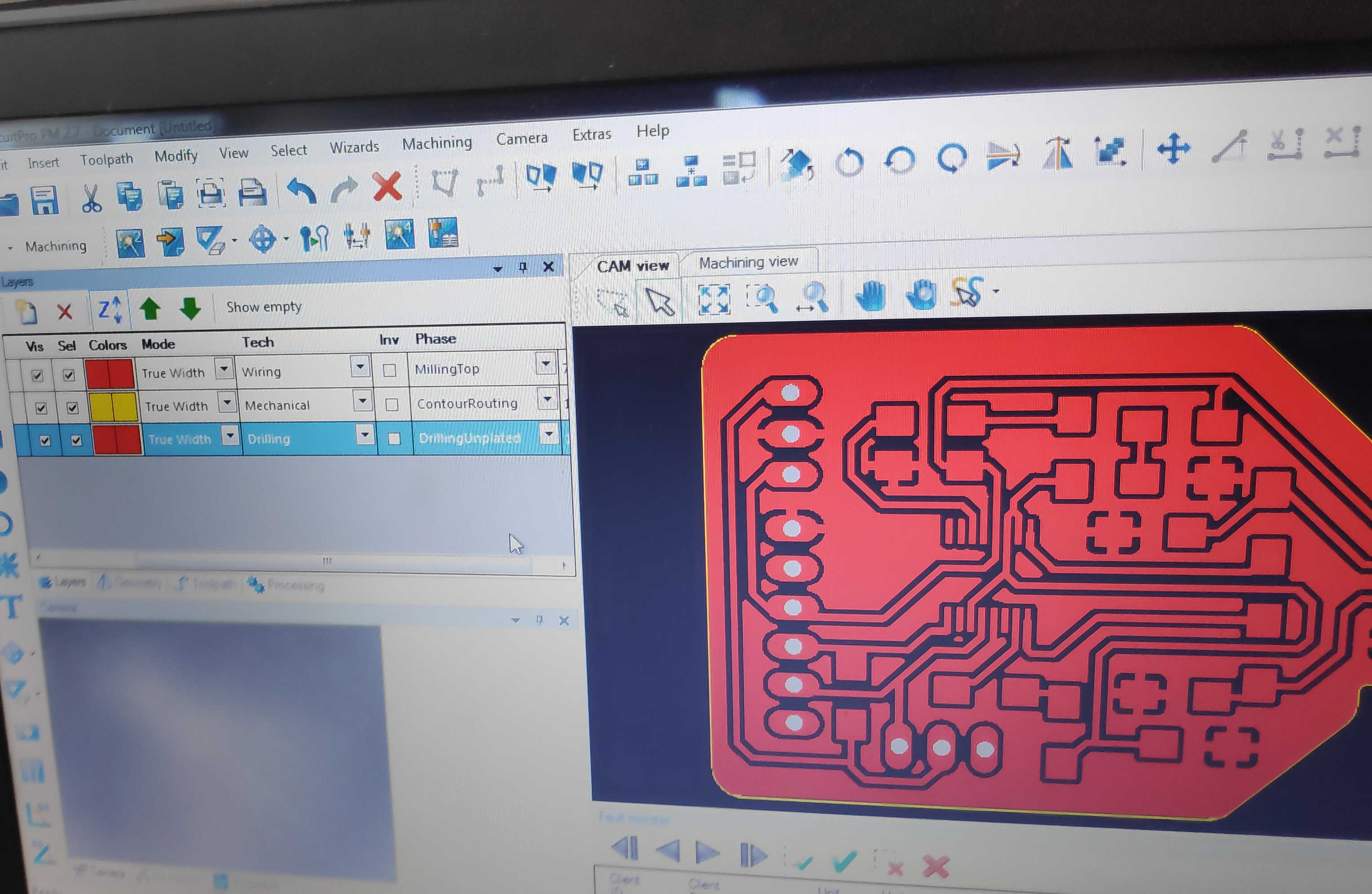
For the next step the file needs to be imported into the CNC-Software. I used “LPKF Cicuit Pro”and import the created .drl, F_Cu.gbr and Edge_Cuts.gbr files. Check if the units are still the same and all import files are marked active. By pressing ok, a window with templates will appear. Select Single Side top to only cut the board from above, which allows it to place component on the top of the board. In the layer-list change the settings for drill job under “tech” to drilling and “phase” to DrillingUnplated. If the files are imported correctly, the PBS board line layout should be visible and colored based on the manufacturing job.
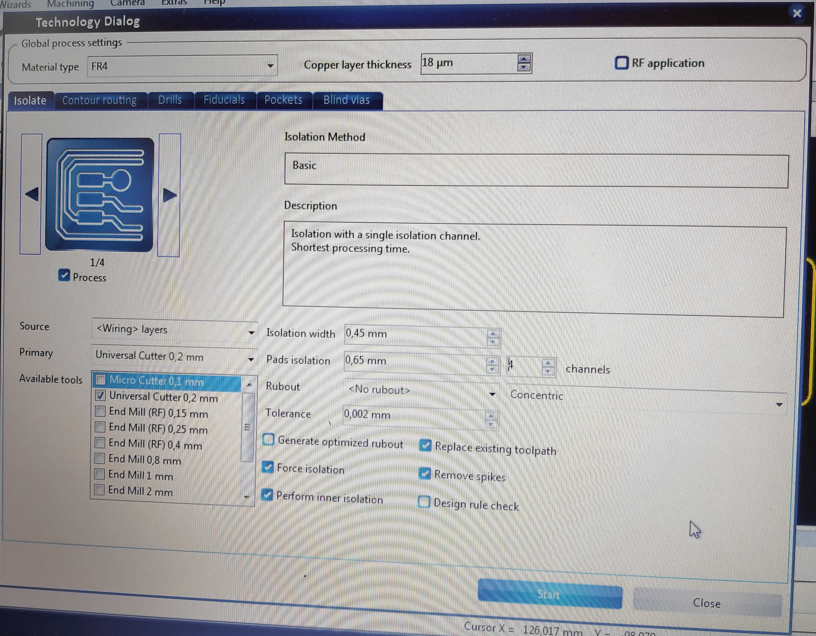
Press the “technology dialog” button to configure the front cutout Job and the edge cutout job. Starting with the Front Cutout Job (Circuit itself) select the drill bit for removel. Select the “Universal Cutter 0.2mm” and deselected all other drill bits. Set the isolation width to 0.45 mm and the channels to 4. Than select the process on how much material should be removed. I used the Type 1(Basic), which only removes material around the lanes.
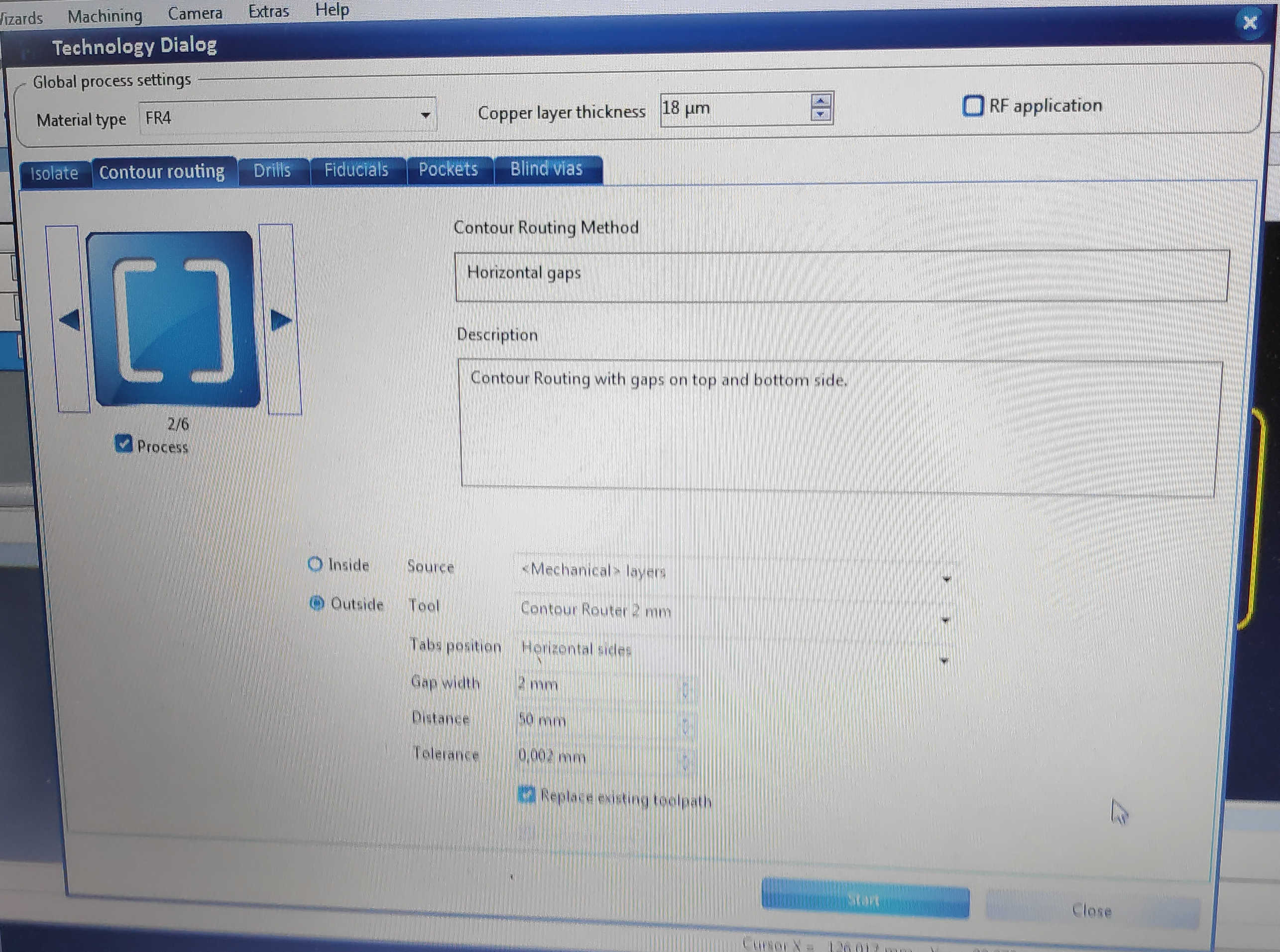
For the Contour routing select method 2-3 depending on whats easier to remove. Both methods leave only to connections to the cutout material. Gap width should can be set around 2mm. When the configuration is finished press start.
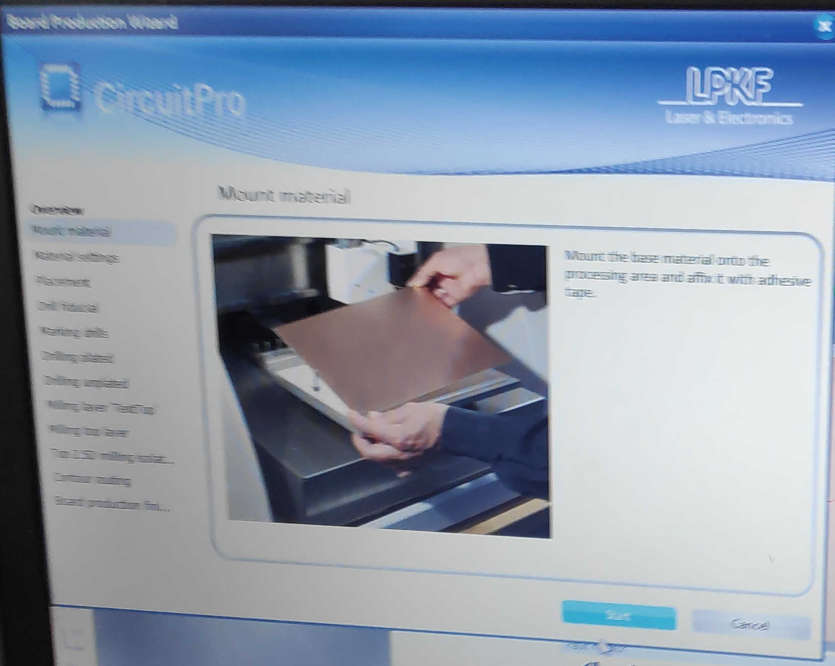
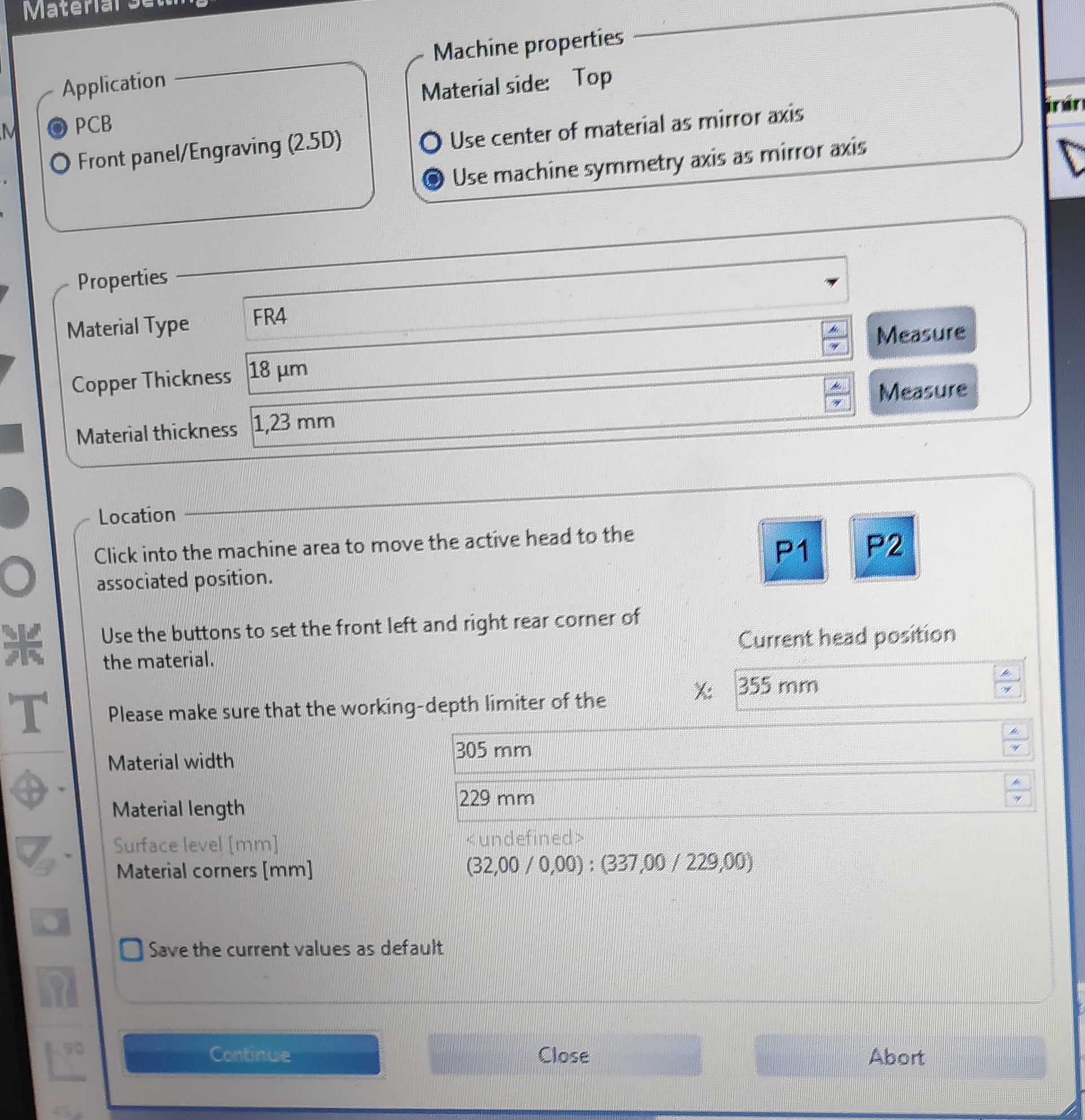
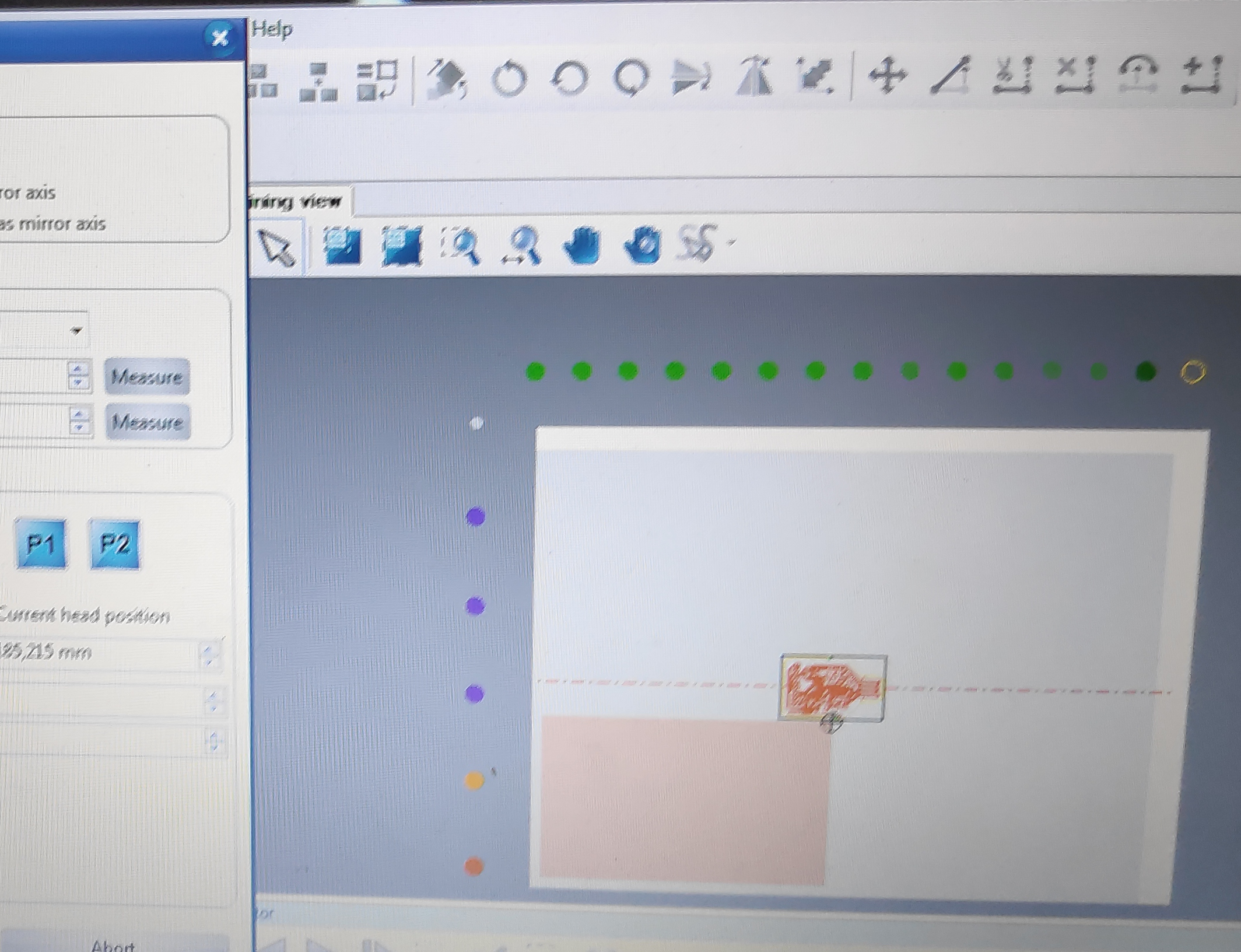
Now just open the “Board Production Wizard”, which will guid through the next steps. Mount the wanted Circuit material on the base of the CNC. The PCB material can be glued on the cutting table with adhesive tape. Press start on the “Board Production” window, if the material is aligned with the corner of the CNC. This will open the configuration for the used material. I used FR4 with a Copper Layer Thickness of 18 μm and a material thickness about 1.23mm. Next is the configuration of the location of the PCB material on the Table. Use the mouse on the left window after pressing p1 to set the first and p2 for the second corner. This will move the drill head to the point. Both points define the height and width of the material. Pressing continue to place the board on the PCB material and define the amount in the x and y direction. For more cut precision use the “Material Auto-Leveler” tool for compensation. Moving to the next step will start the drilling process. This process might take a while because the motor first needs to heat up and has to pick up the wanted tool bit.
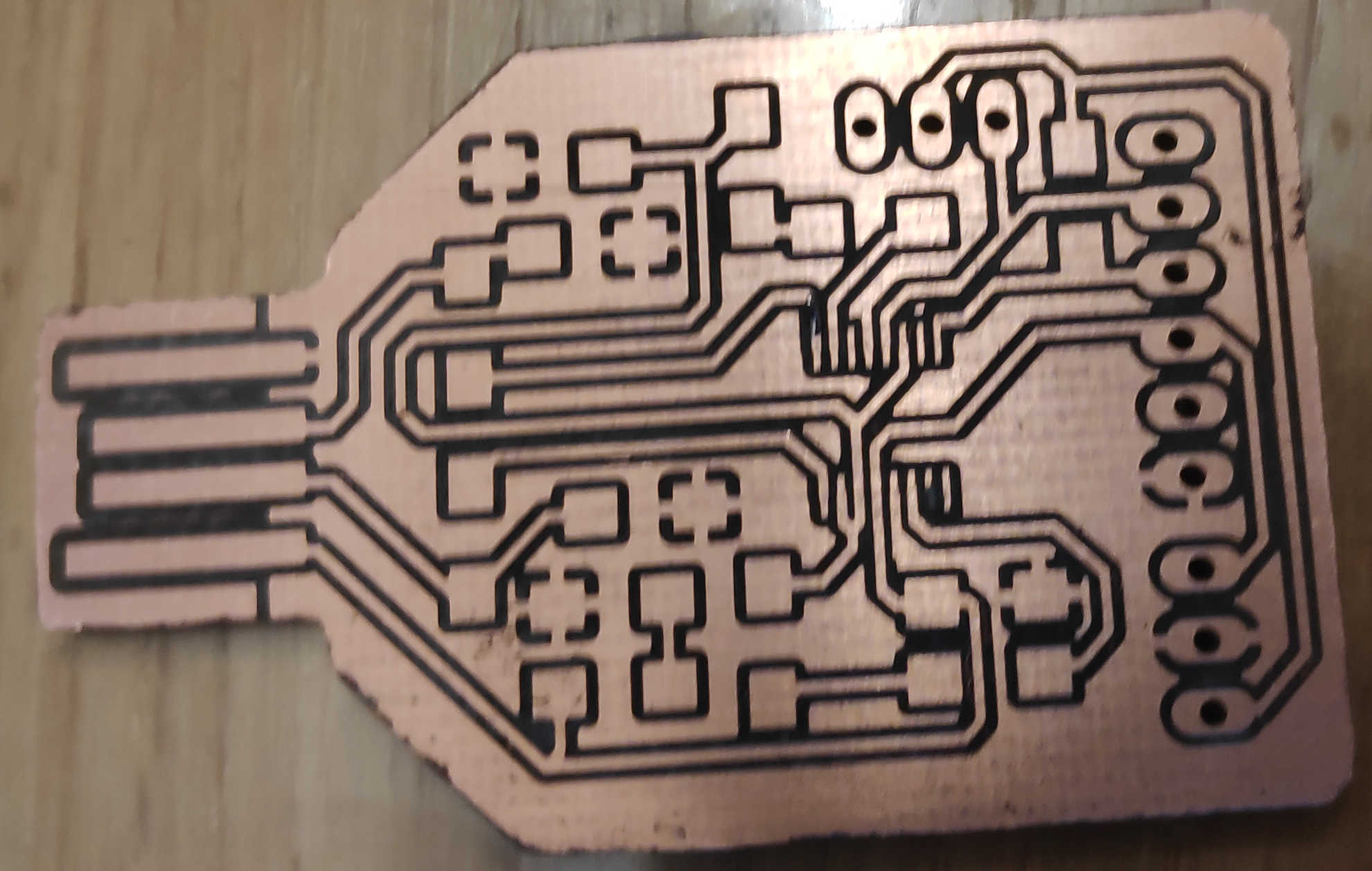
The finished result should look like this.
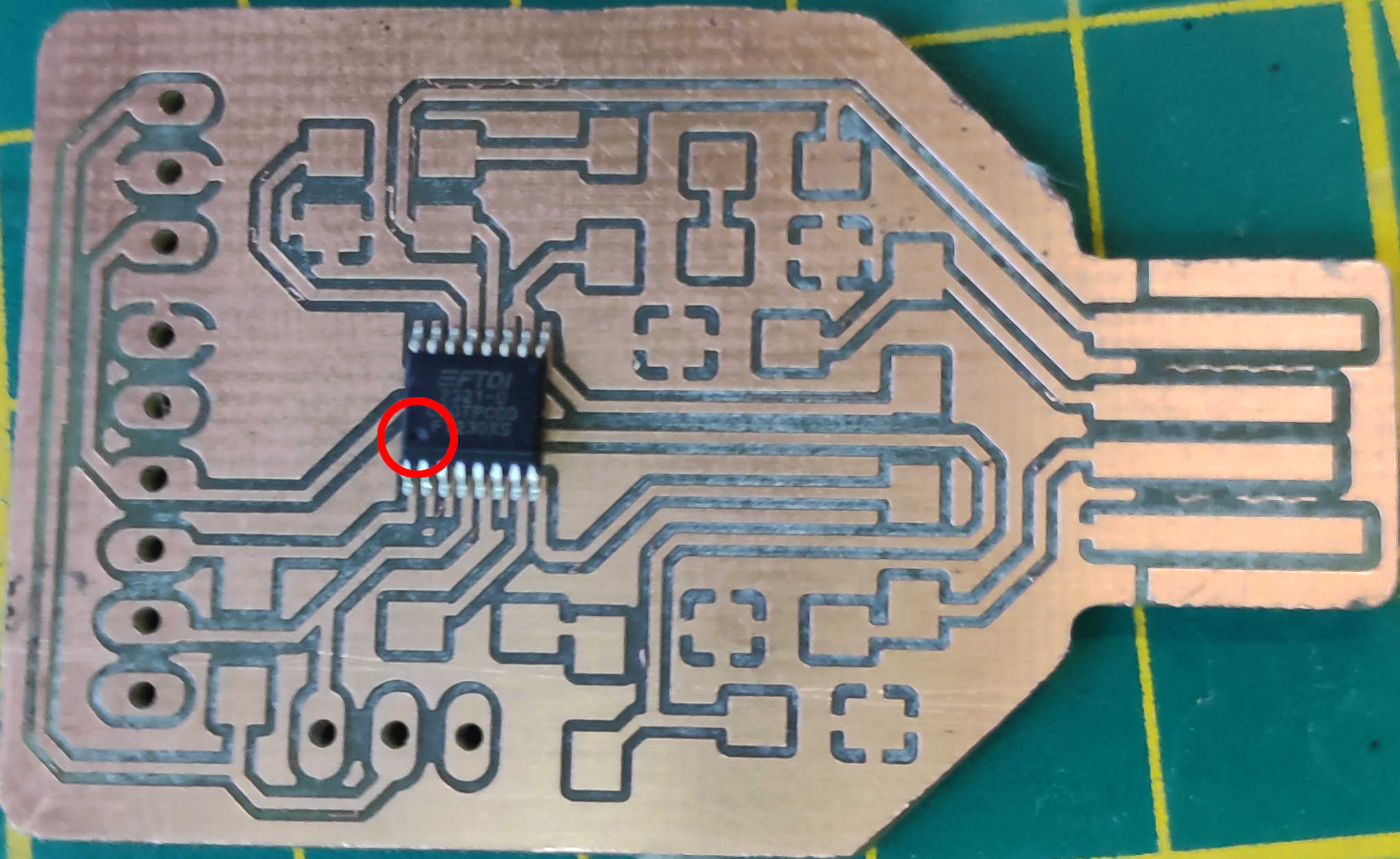
Than the components needs to be placed on the PCB board. Use the list provided from the link to check, what electronics components are needed. Most of the components are Surface-mounted, so soldering is done from the top. For the mounting reference I used the layout provided from the .kicad_pcb file. My board had some protective coating against UV on it, which I removed with acetone before soldering. A rule of thumb is to start soldering from the inside out. I started with the chip in the middle, which was also the hardest device to solder on this board. To solder the small pins to the board use very little solder. Apply it first on one of the outer lanes on the board and place the controller carefully on the board, while still heating up the solder. To place it the right way, the chip indent point needs to be aligned with cut-off edge from the layout. Fixate the diagonal outer pins to align the whole controller on the board. Now the rest of the pins can be solder to the board. Use solder as less as possible. If its bridging two pins on the chip use a bit of flux and desoldering braids to remove it.
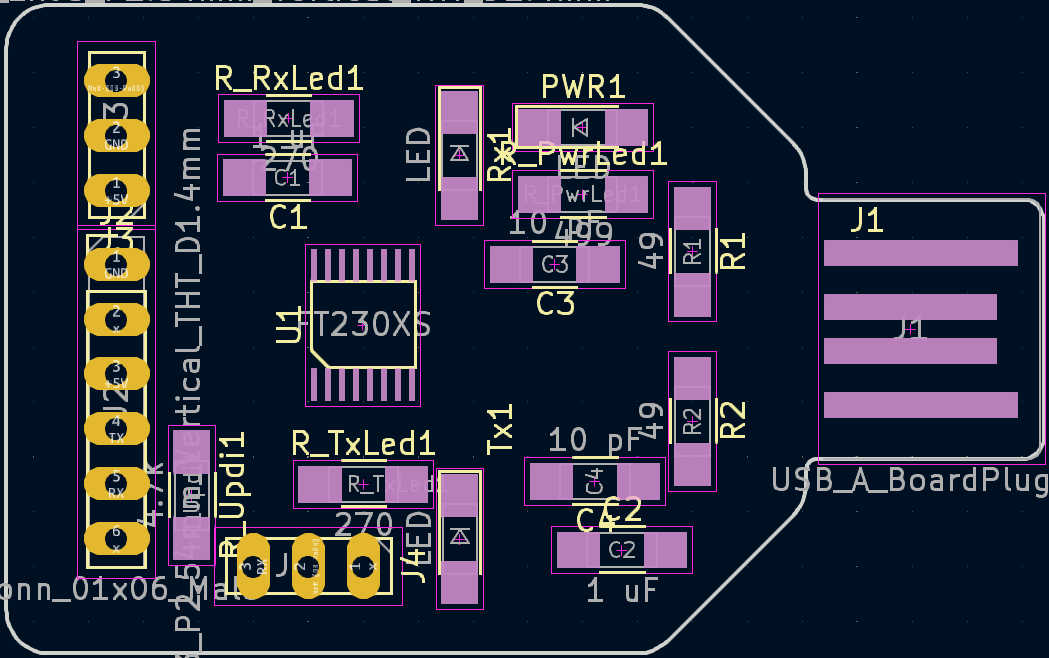
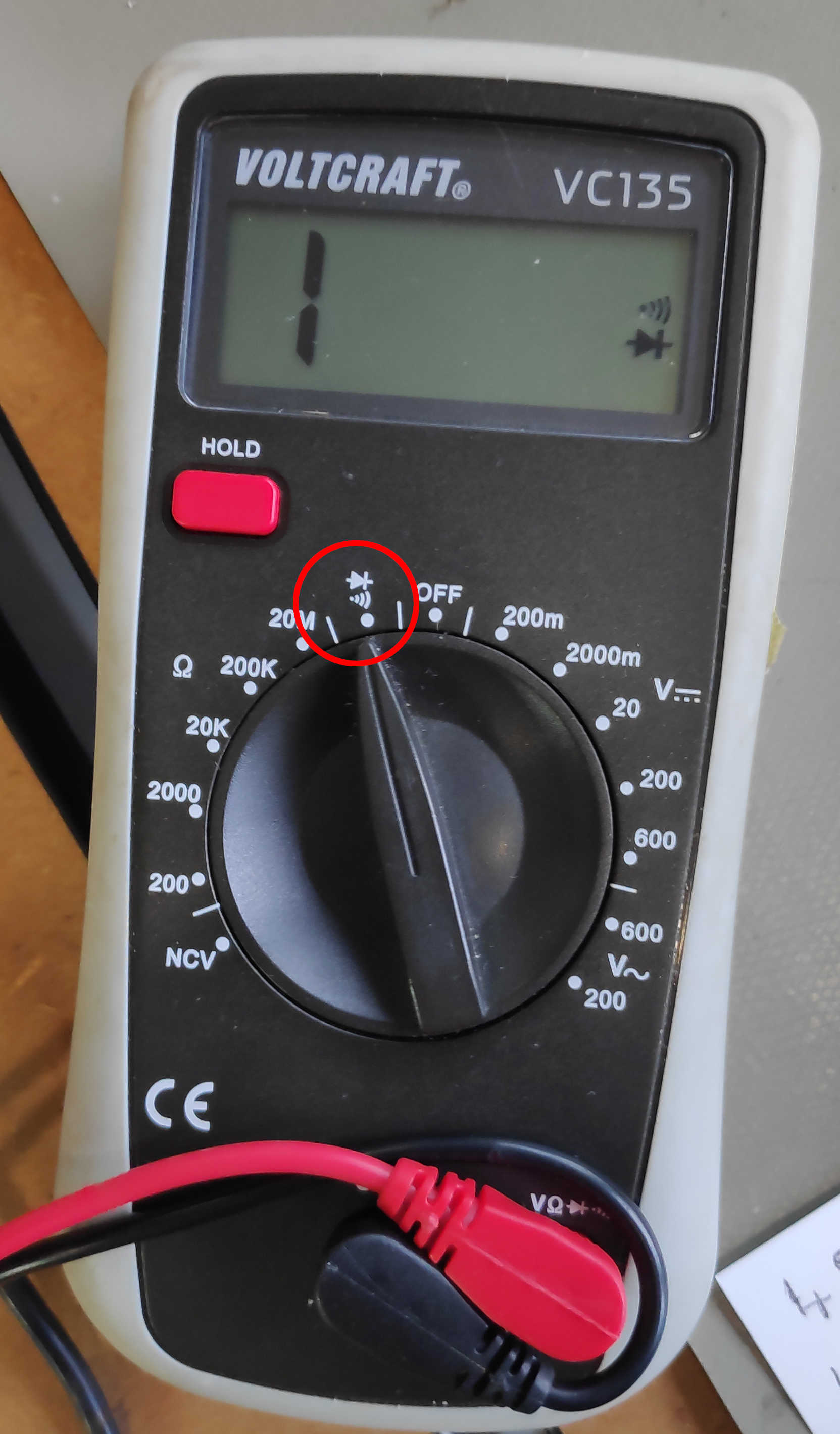
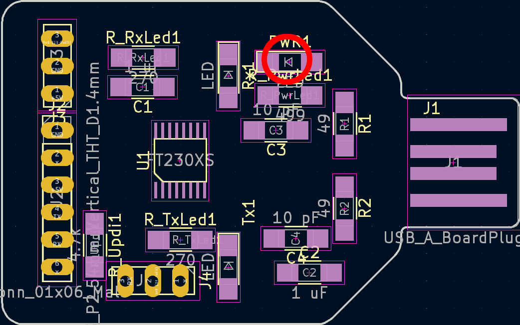
Next components are the resistors and capacitors. Both components select for this board don’t have current float direction, thus it won’t matter which way they are turned. To solder the LEDs onto the board, the direction is important however. Use a multimeter or the arrow at the backside to determent the direction of the flow. Testing the direction of the LED with a multimeter, using the continuity tester with the LED. The LED should light up, if the VCC and GND is on the right side. Use the arrow on layout, which points in the current flow direction, to align the LED.
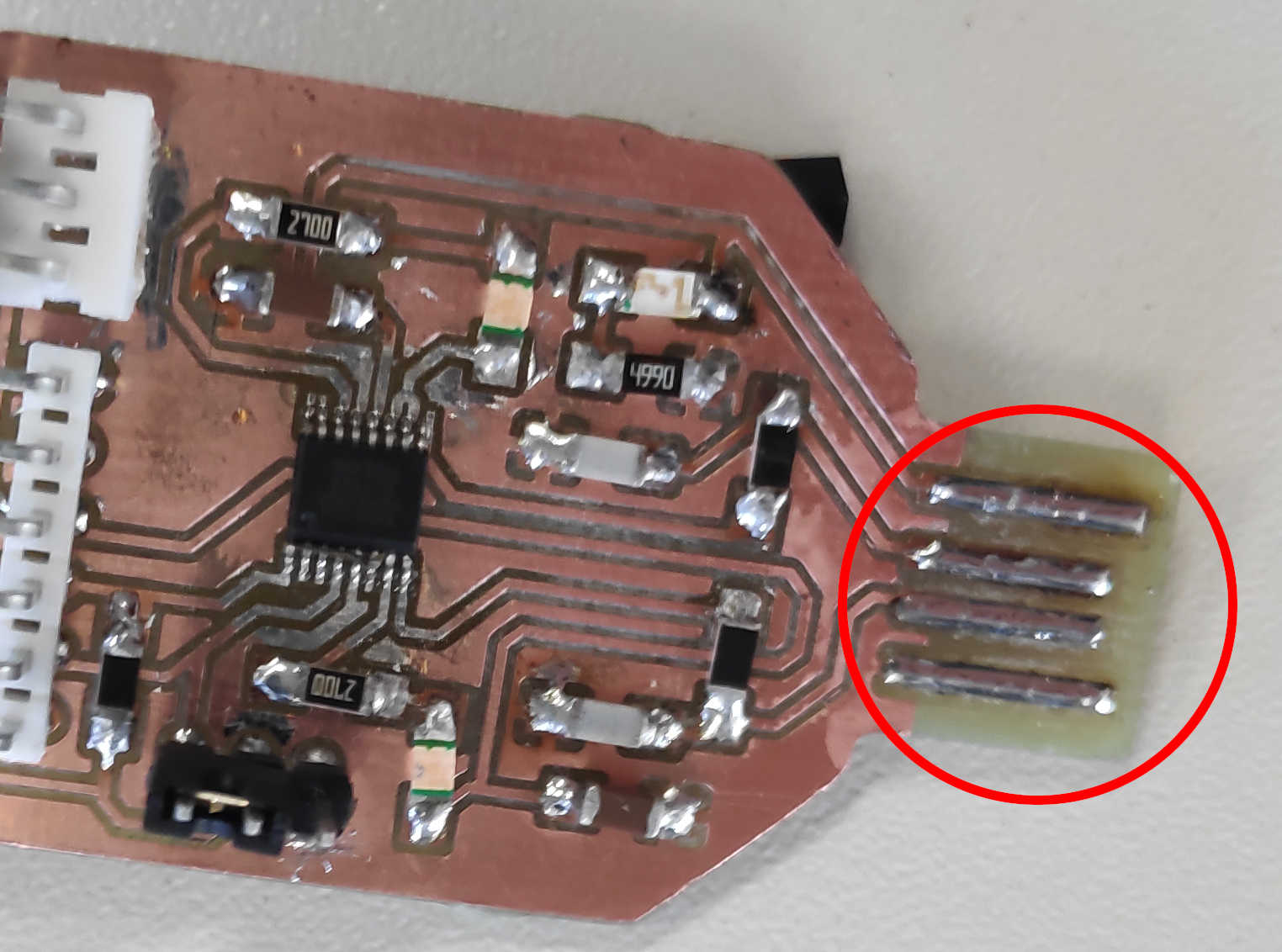
For adding the Pin header to the board pull them high up as possible, to have enough space to solder under the plastic covering of the pins. Touching the pins with a little bit of solder on both sides will be enough to connect it. Lastly to make the USB connector better accessible add solder evenly by using flux on the USB lanes. Remove any copper leftover, which aren't connected to any lane to prevent damaging USB ports.
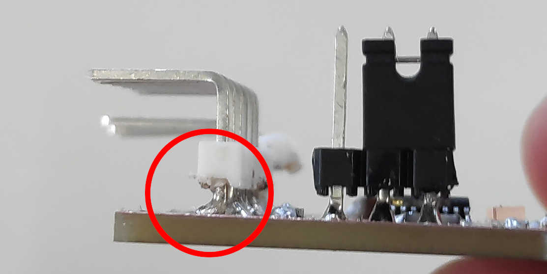
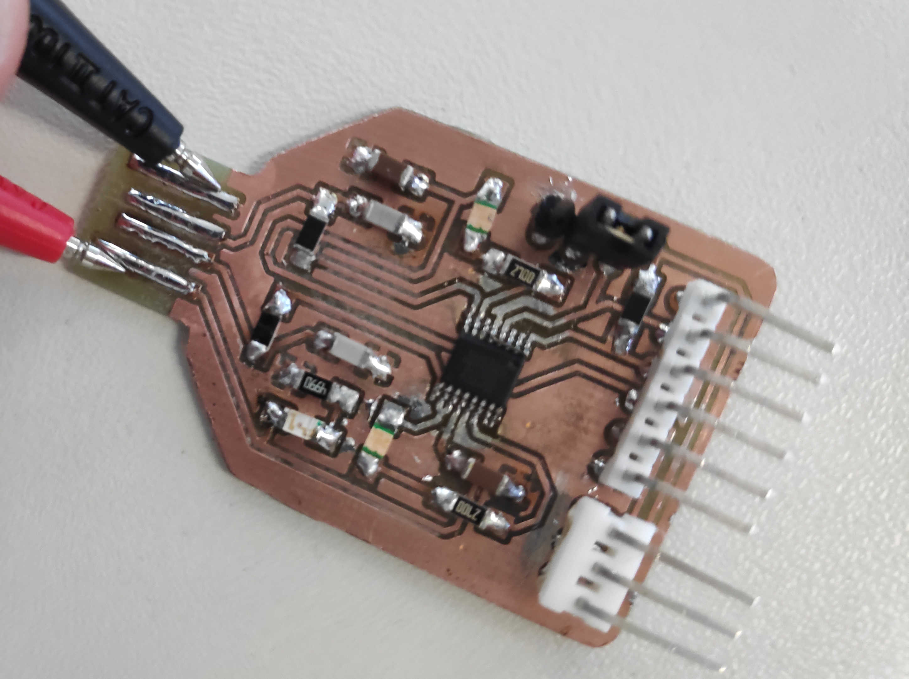
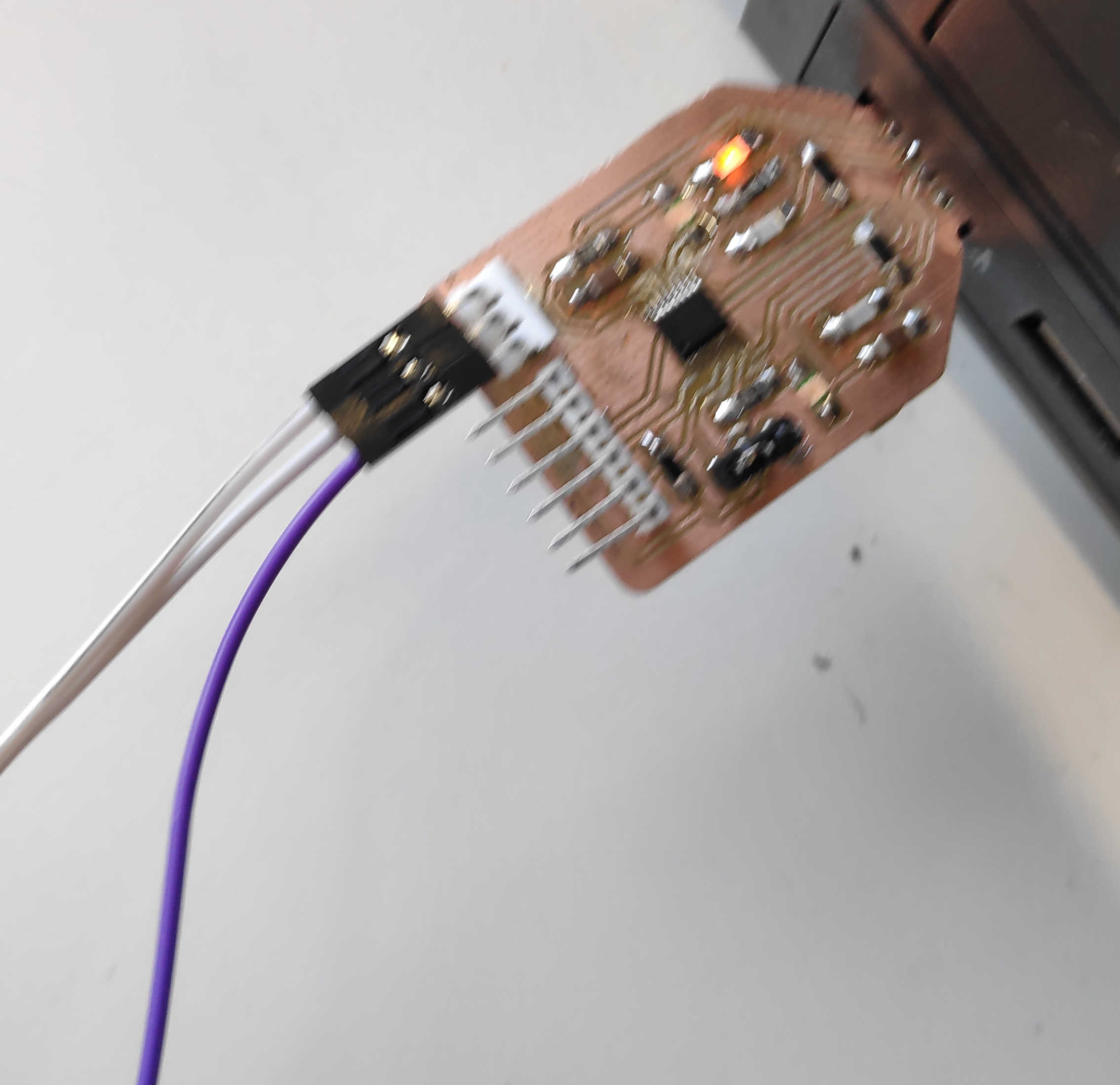
Lastly test the board using a multimeter continuity tester. Put on the jumper to set the board to programming mode. Put the GND of the multimeter at the lane and the VCC cable at microcontroller corresponding Pin. If the multimeter beeps or blinks, that means that the connection is working. Furthermore check the pin heads for to each lane. Same as above it should beep if the pin header is connected to the board below. Lastly the connection of the USB needs to be tested. Put the multimeter GND on the USB GND pin and VCC on the USB Vcc. It should not return a beep, because the resistors should eliminate any current running through the board to the GND. If there is any lane bridged due to solder making a connection, fix it by using desoldering braids to remove it. In my case the power LED wasn’t all the way on both pads, which created a short circuit.When all lanes are connected right, the USB connection can be tested. Plug the Board all the way in. Keep in mind to use a USB hub instead of connecting it directly to a pc, thus now usb ports getting damaged. If the power LED lights up, that mean that VCC and GND was connected successful.
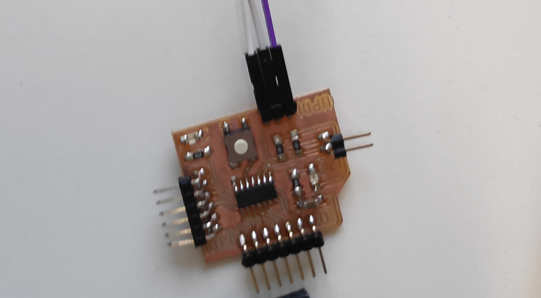
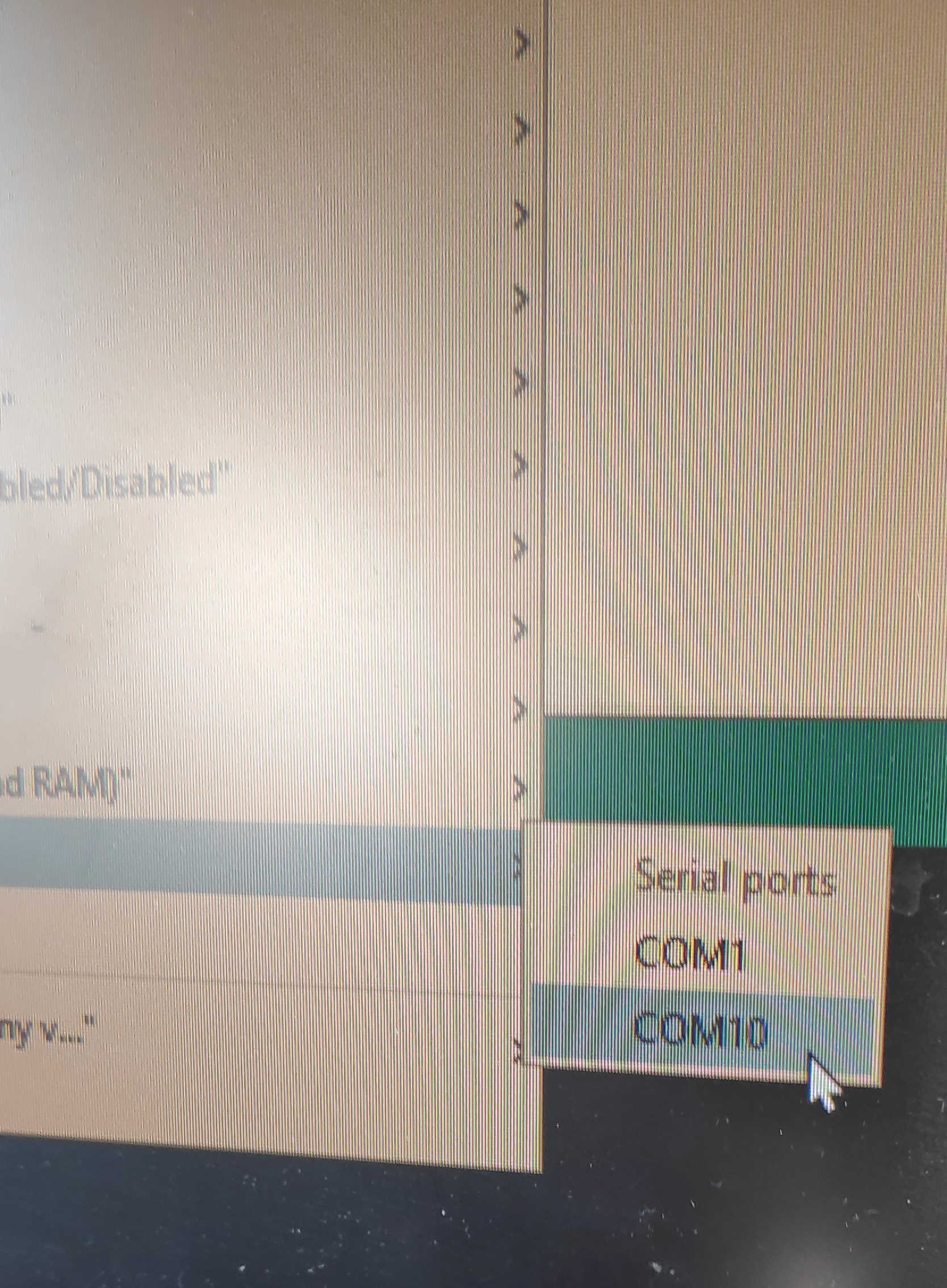
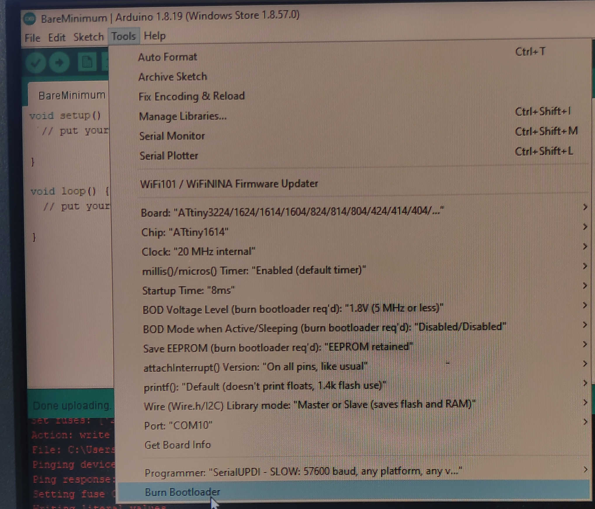
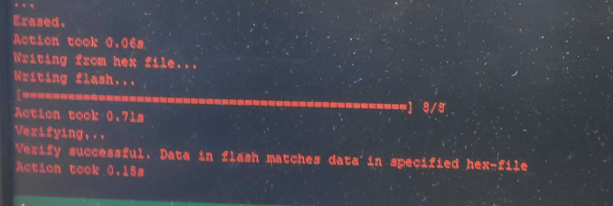
The writing function can be tested by wiring the 3 pins from the pin header with a test-board of you choice. The middle Pin should be GND, the most outer pin is Data pin and other pin is VCC. To test the writing Mechanism I opened Arduino IDE to flash the selected test-board. I than loaded a simple programm and selected the USB as a new COM. The test-board can now be flashed by going under tools > burn bootloader. This will transmit the data to the test-board and open the console to inform about the current status of the flashing. The Tx1 and Rx1 LEDs both should be flashing, while data is transmitted. If the transmission was successful, the terminal show it.
Here are the following files used: