Week 10 – Circuit Design
This week assignment builds on top from last to weeks. The task was to design a circuit for the “ATtiny” Chip, which can be later used for the final project. Furthermore this board needed to be manufactured and solder.
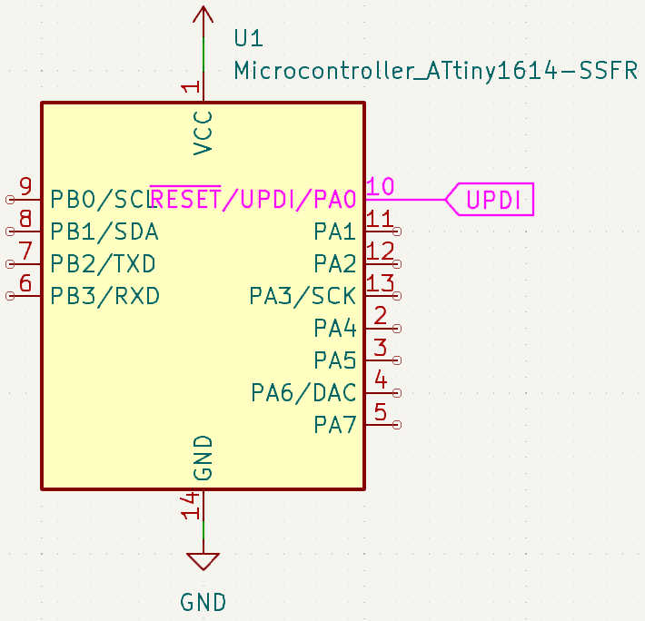
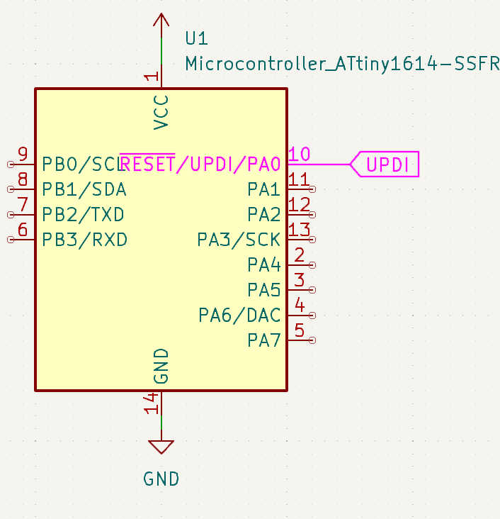
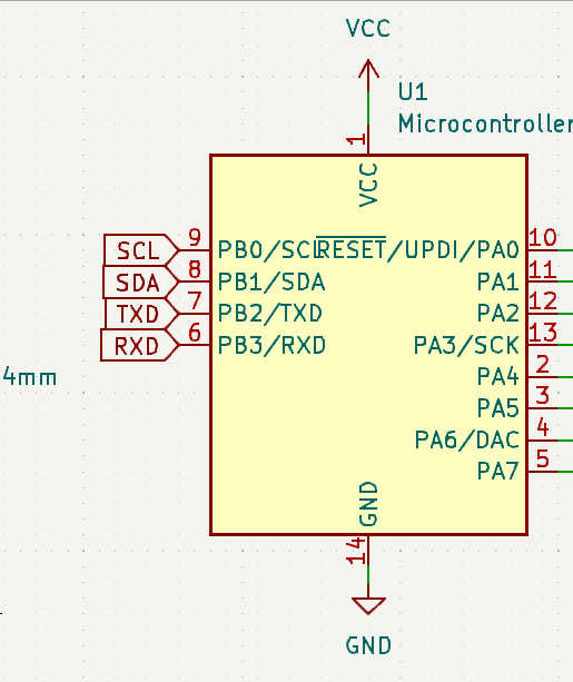
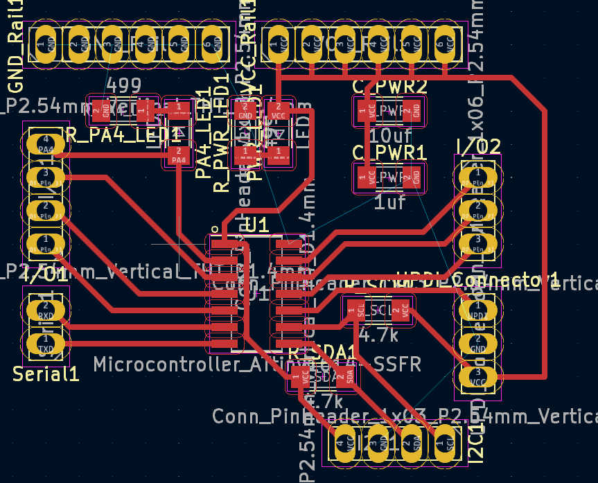
Of curse the first step was to create a design. In this step, I began noting down what components I would need for the final project. With this rough list of the component I estimate the pins in needed to use. For my project I need a I2C connector for a display (SCL, SDA), 2 Digital Pins for a rotatory encoder (A Pin. B Pin), 4 Buttons each assigned 1 digital pin and an analog pin for the speaker (PWM). Looking at the design of the alarm clock, it was clear that one board can’t cover all positions of input devices. So I needed to design a generic board on, which I can connect my devices.
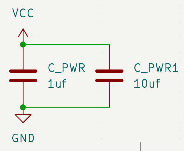
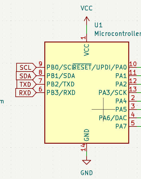
I did the design in “KiCad” by creating a new Project, which allows me to update the layout while editing the circuits diagram. I began by placing the ATtiny1614 from the symbol library in the circuit diagram. If the “ATtiny” doesn't appear an installation of the library is needed. Connect GND and VCC of the “ATtiny” to the GND and VCC using there symboles or use a tag. To give the controller a smooth electricity flow, connect 2 Capacitor between VCC and GND, one 1μf and one 10μf.
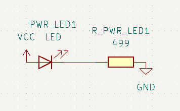
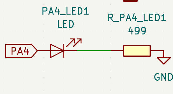
To check if the board is active connect a PWR-LED with a resistor (in this case a 499Ω) between VCC and GND. Make sure that the LED shows in the direction of the electricity flow.
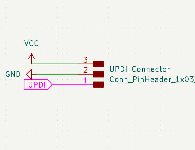
Next up is the UPDI connector, which uses GND, VCC and a UPDI pin. Checking the datasheet of the “ATtiny” reveals that the UPDI Pin for this model is on PA0. Create a 1x3 pinheader from the menu and add GND as middle, VCC and UPDI as outer pins. Using the tag feature the pinheader doesen’t need to be directly connected in the diagram, but can use this tag as a reference to the UPDI pin.
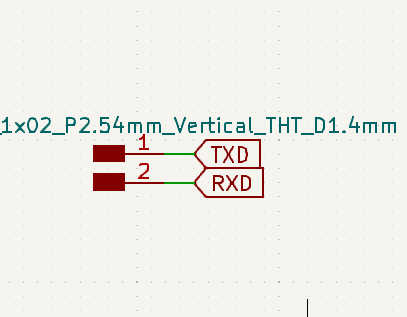
For the serial connection pins, just connect a 1x2 pinheader with TxD and RxD Tags, which are also connected to the board.
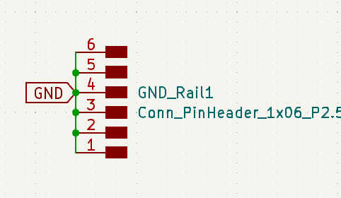
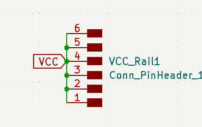
To have more GND and VCC available just connect rails to each one. To create a ground rail, connect the GND to a 1x6 pinheader, where every Pin is connected to the GND. The same design is used for the VCC rail, but instead uses VCC as a connection.
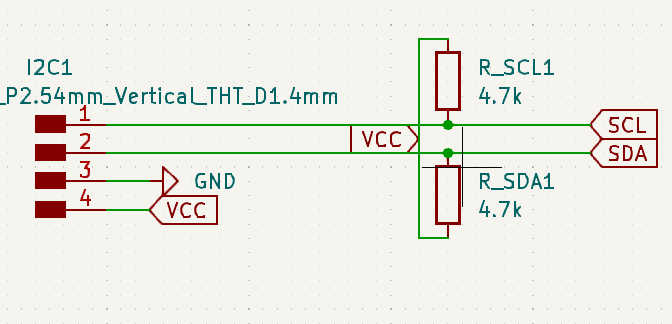
For the I2C the connection is a bit more complicated. Each I2C pin works like a switch, which can be turned on or off. To prevent floating, a pull-up resistor is needed for each pin. Connect VCC with a big resistor (4.7kOhm) to the board. The SCL and SDA can than be connected to the 1x4 or 1x2 Pinheader depending, if VCC and GND should on the same pinheader.
The leftover Pins also needed to be connected to the pinheader. In this case “ATtiny” pins 2 -5 lie on the other side than the rest, thus the pinheader needed to be split into two. For the pins 2-5 I used a 1x4 pinheader and for the 11- 13 a 1x3 pinheader. Each pin can be just connected to each pinheader.
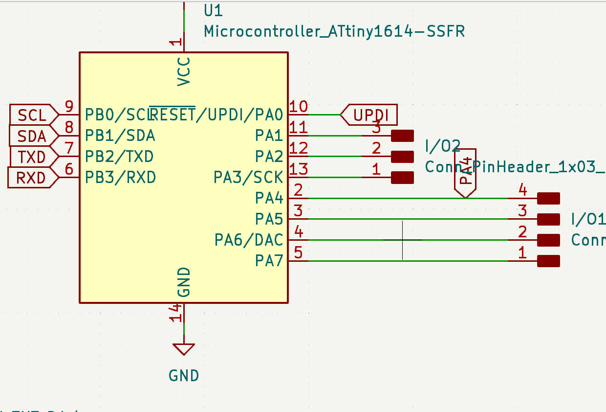
Lastly a LED needs to be connected to a pin to finish of the Assignment. I selected pin PA4 and connected it parallel to the port, thus I doesn't block the float direction of the current.
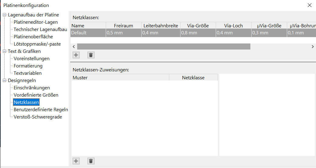
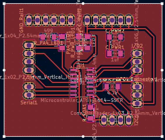
Moving over to the layout design in KiCad, the reference need to be assigned in circuits diagram by opening the annotation window. Afterwards each footprint of the library needs to be assigned to each component. Only if this is done you can move layout design. First update the layout window, which will append the components to the mouse. Place them down so each component can be adjusted. Go to the setup for netclass, to define the thickness of the wires, that will be later used to connect each pin. The space around the lines should be around 0.5mm and the line thickness of about 0.4 mm.
Start the layout by placing each component near it’s pin, which is indicated by a thin line between pin and component. If the lines of a component cross-over, sometimes rotating it will solve the problem. If everything is in place, the adjustment of the board form can be done. The pinheaders should be around the edge of the board and components like LEDs should be inside.
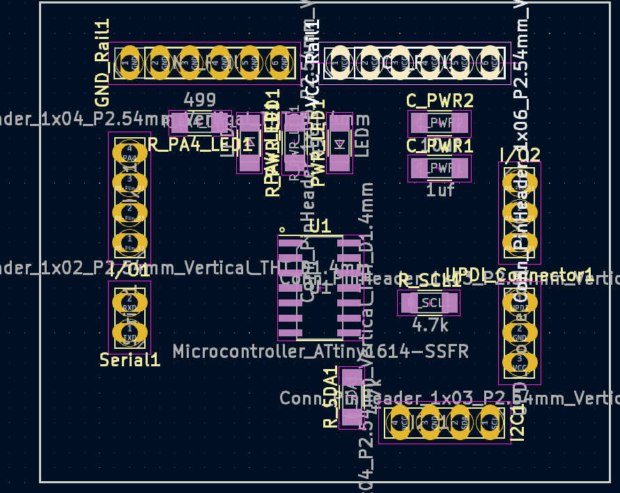
Creating the connection between the chip and the components connected everything except the GND at the moment. Watch out that no drawen lines are crossing each other, because this creates unwanted connections. Second thing to keep in, that straight lines are being used to connect to the chip. Furthermore place the distance between component or lines far apart, so it’s easier to solder. Lines, which creating corners are also unwanted as this can cause jump-over current.
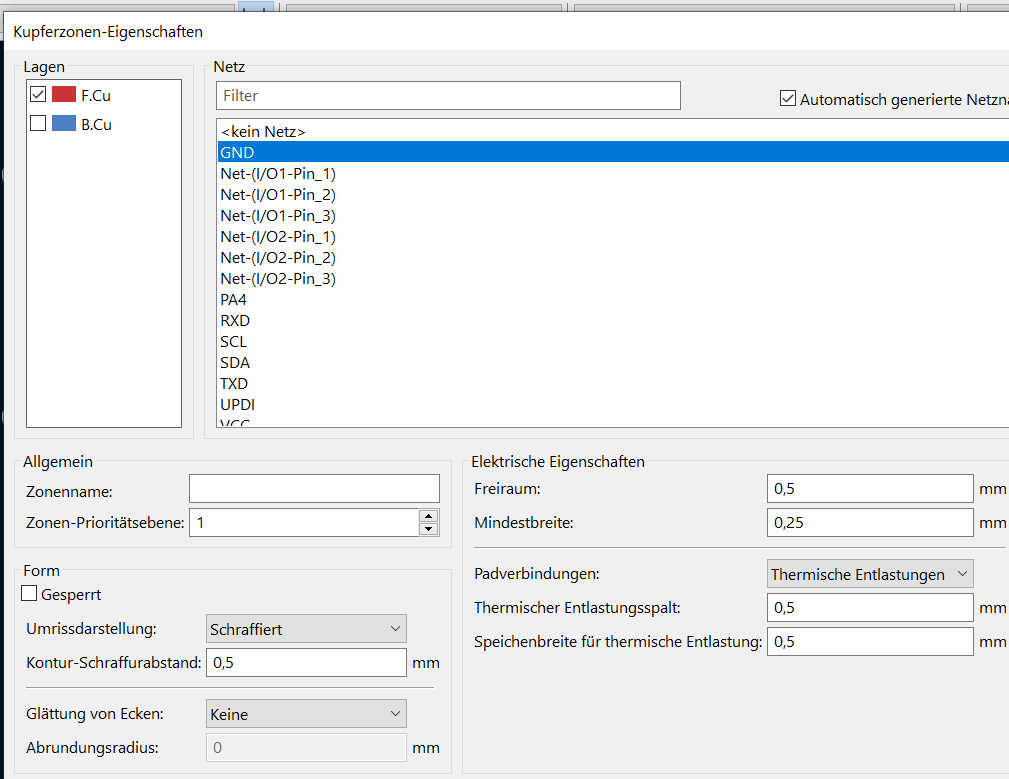
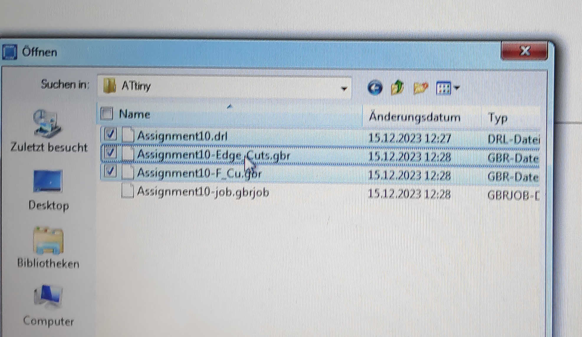
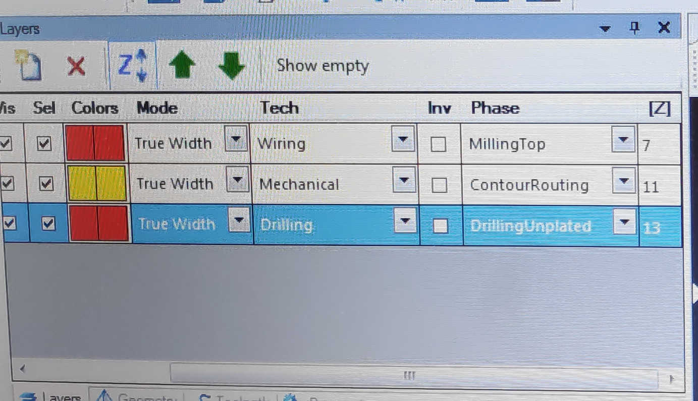
The last step is to connect the GND to the each GND connection. To do this, select add fill-zone and assign the GND to it. This will connect every component, but sometimes the wire configuration will create islands, which needs to be connected back to the GND. To solve this problem, the wire causing this problem needs to moved or replaced with another configuration. Use the rectangle tool to define a rectangle shaped cutout for the board. Now the file can be exported as the weeks before as a gerber files. Needed files are F_Cu.gbr, Edge_Cuts.gbr and the .drl drill file.
Using the CNC , the same process a weeks before can be used. The setting slightly changed due to a thicker copper layer. Start by Important these 3 files and check theme. Then adjust the Drill job, that it will drill instead of being undefined.
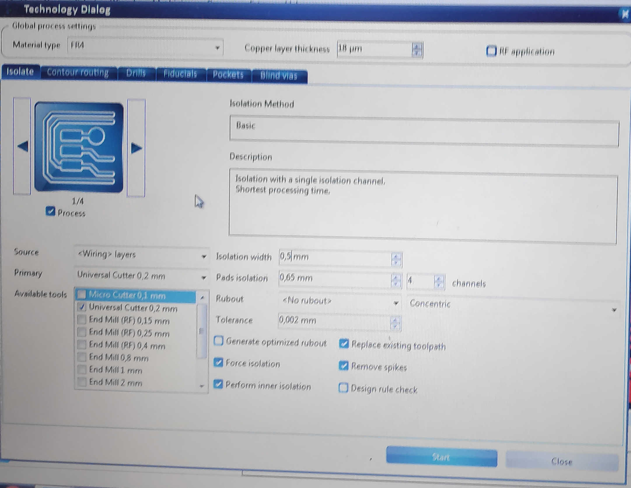
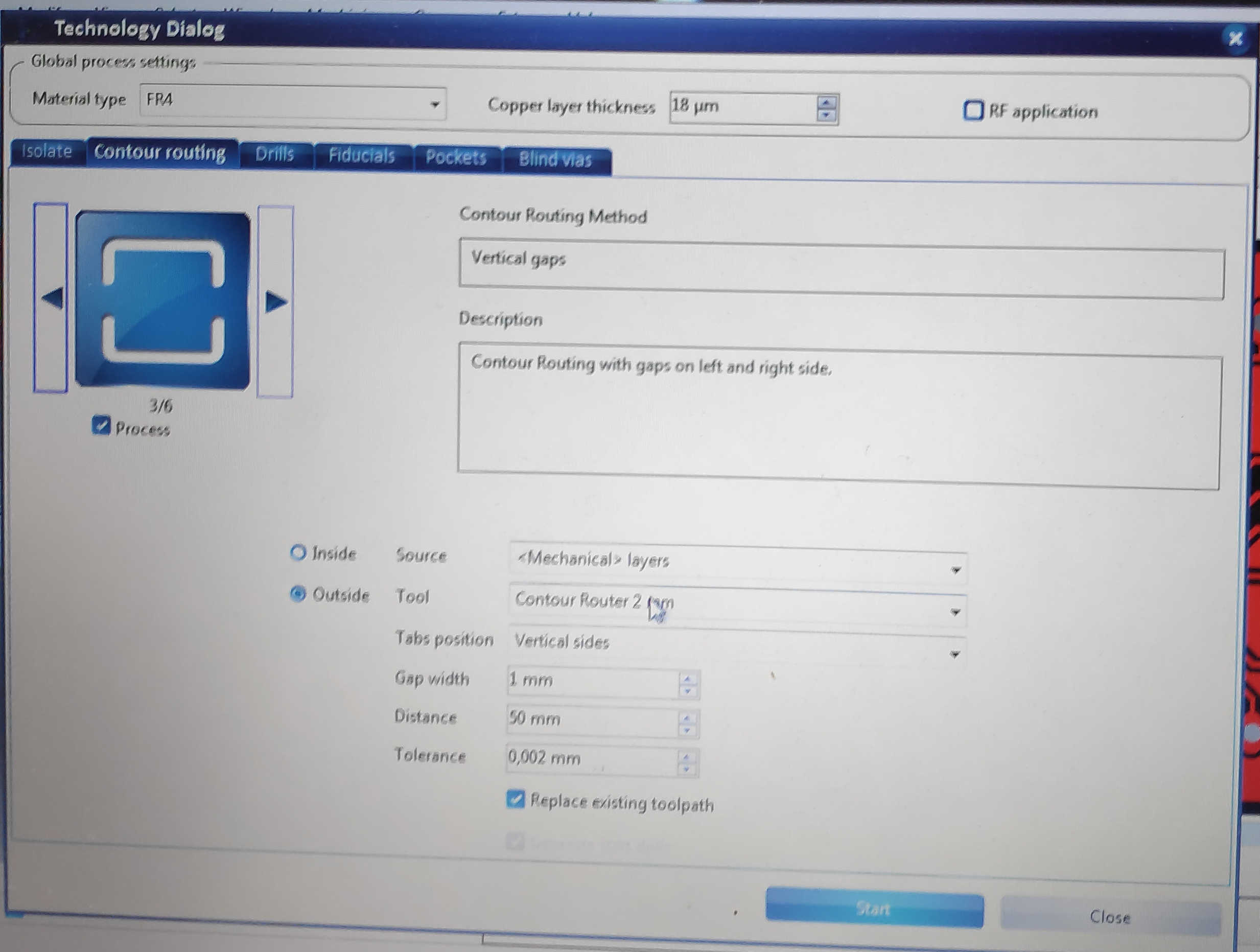
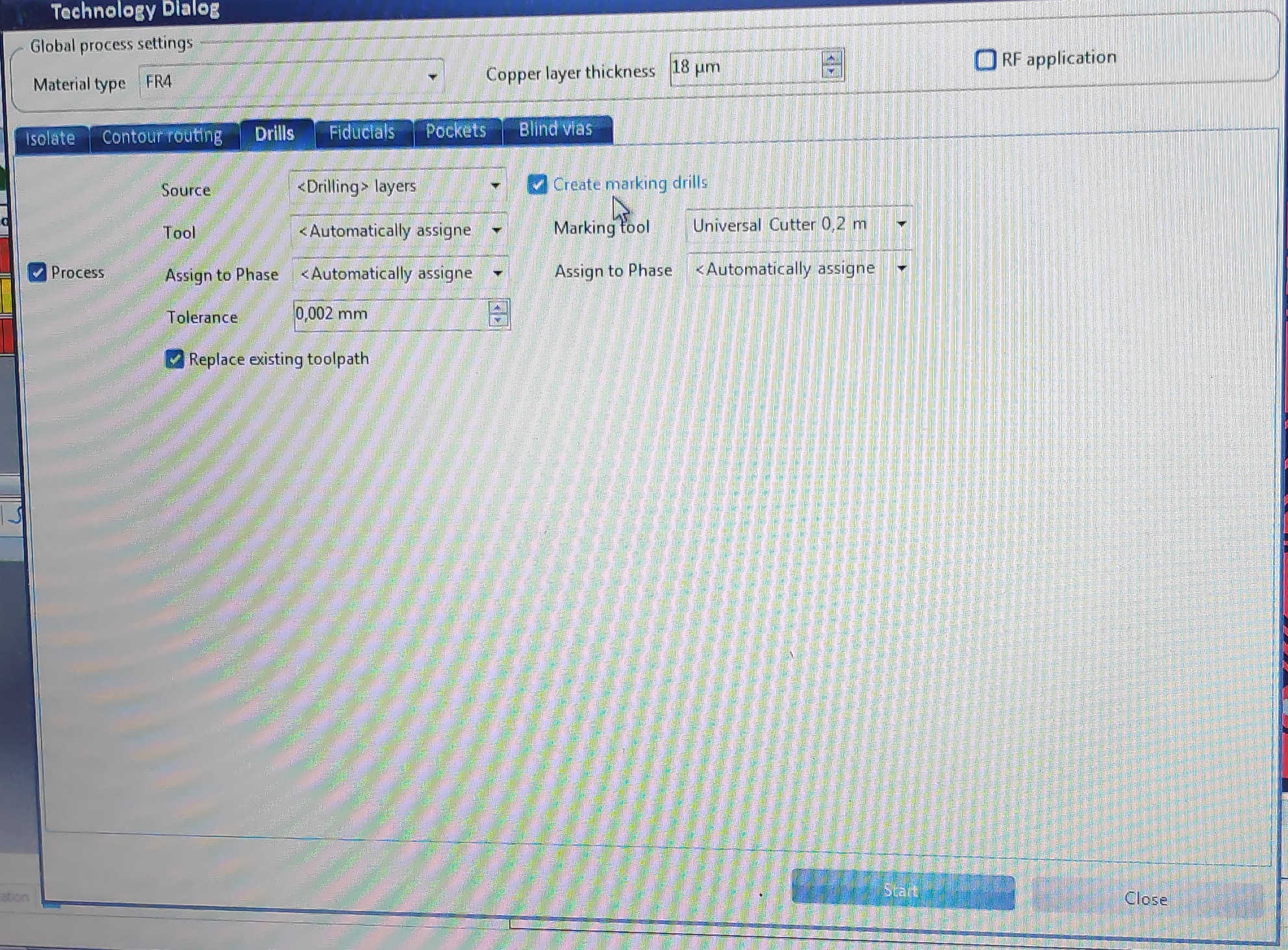
Open the “technologies dialog” and set the type of the Isolation to Basic and only activate the universal cutter. Set isolation to 0.5m and pad isolation to 0.65mm. Switch to contour-routing and select the vertical gap as Method. Check if cut still happens outside the board and adjust the contour size to 2mm. Check if the drill configuration are good. I used the default setting for the drill. Check in the computation Result window, which appears at the end, if all configuration are set as wanted.
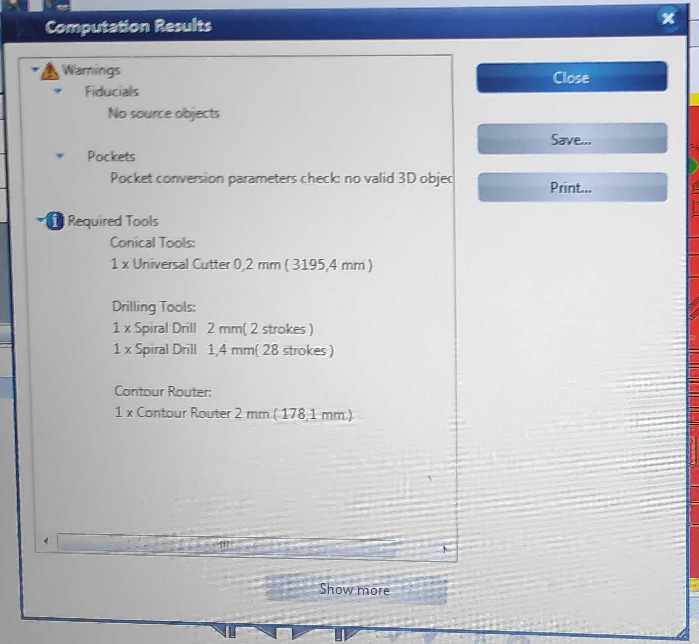
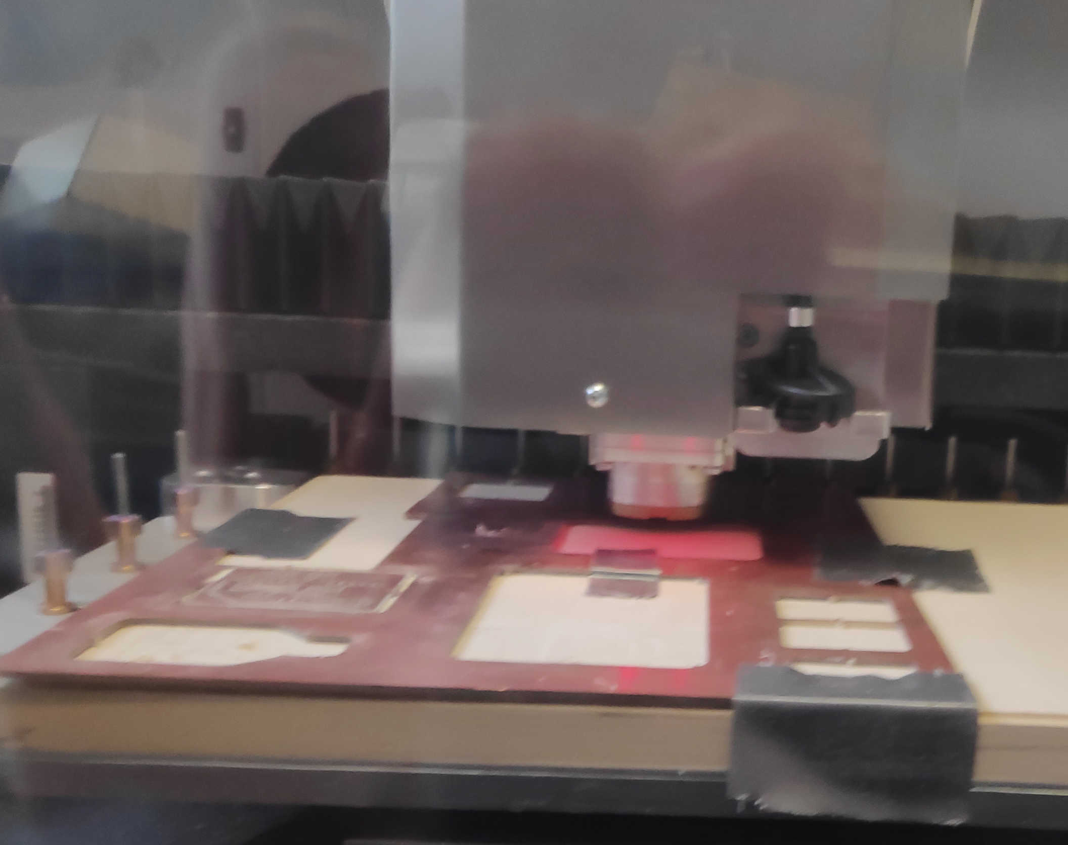
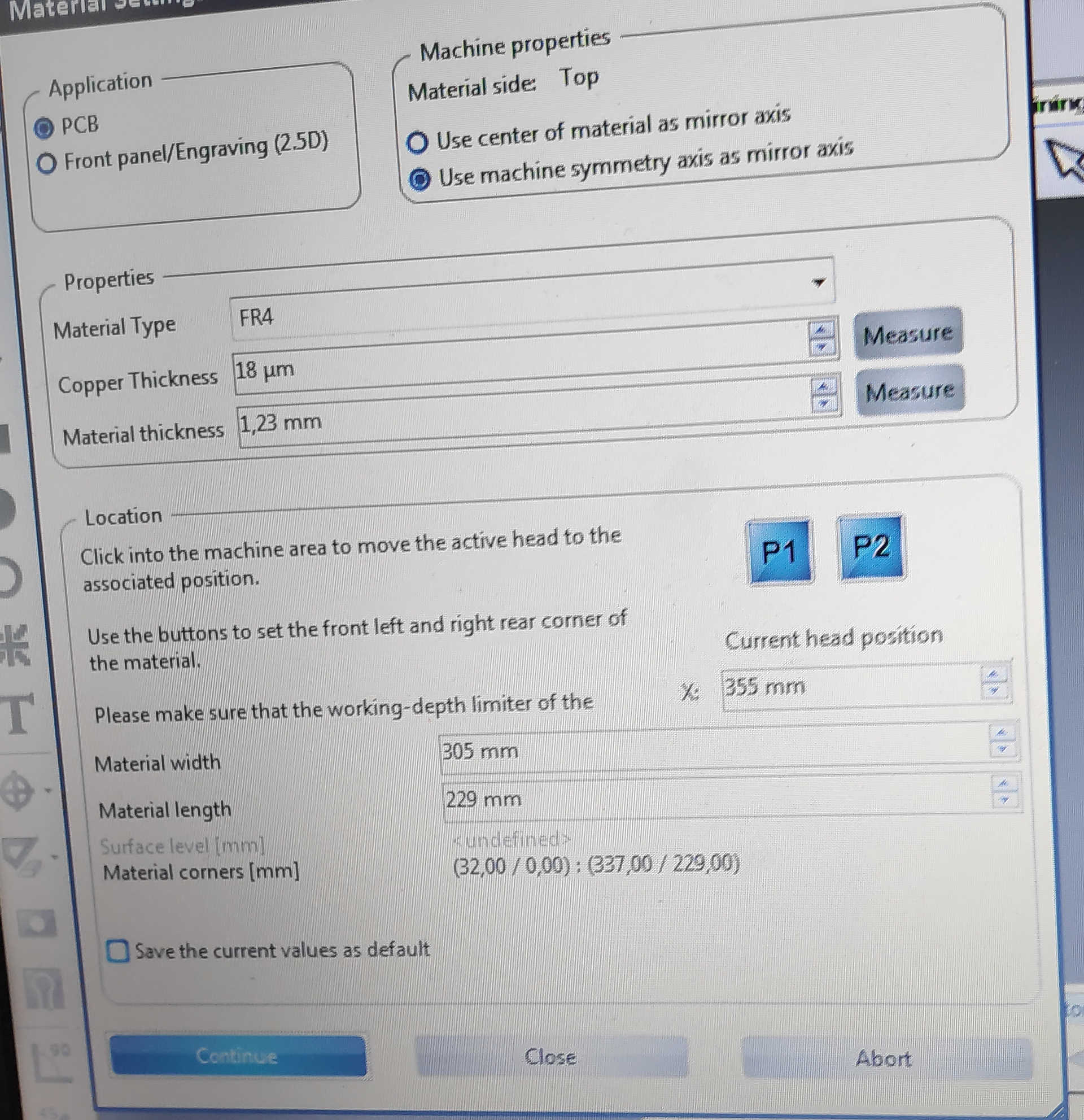
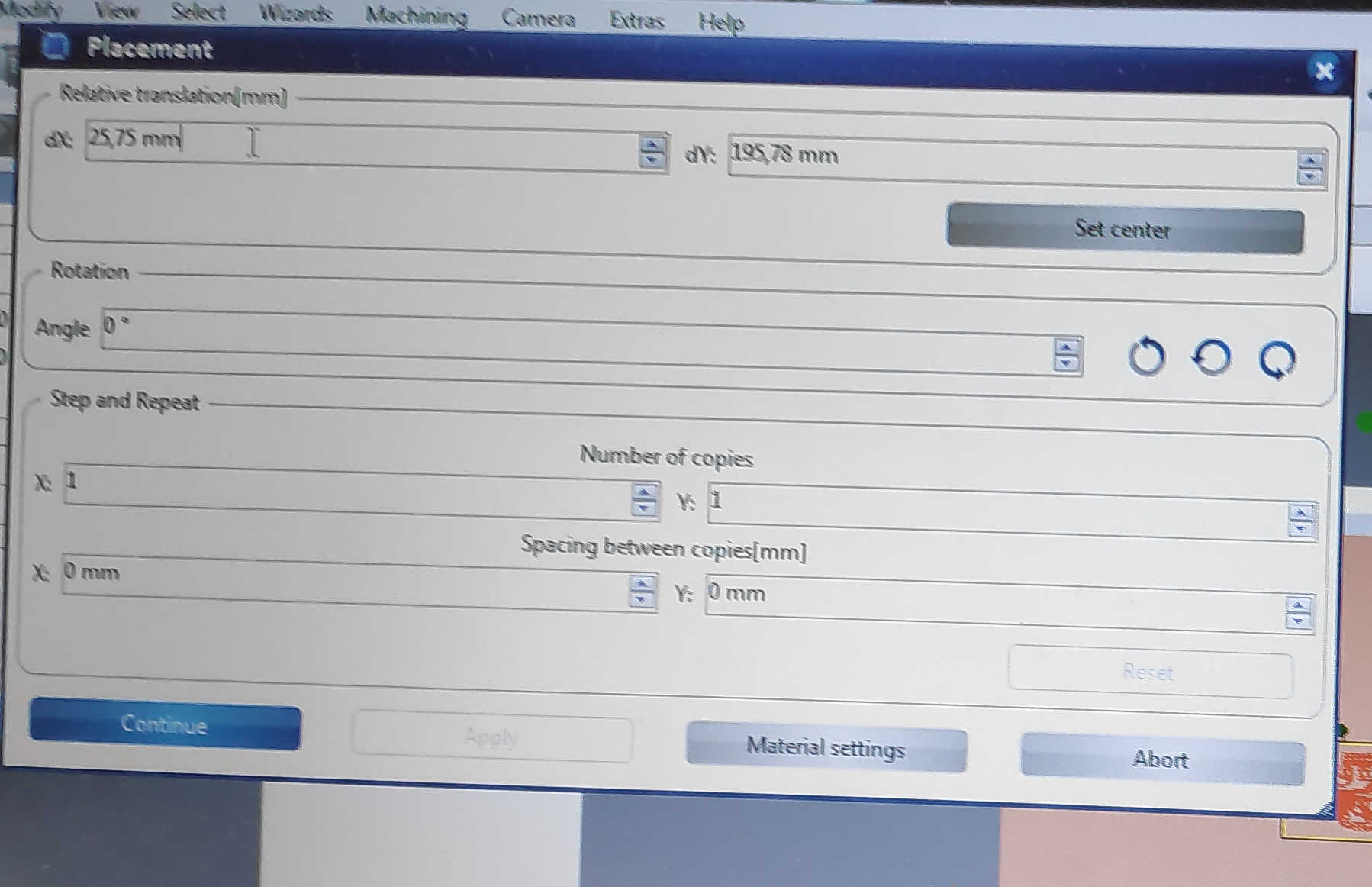
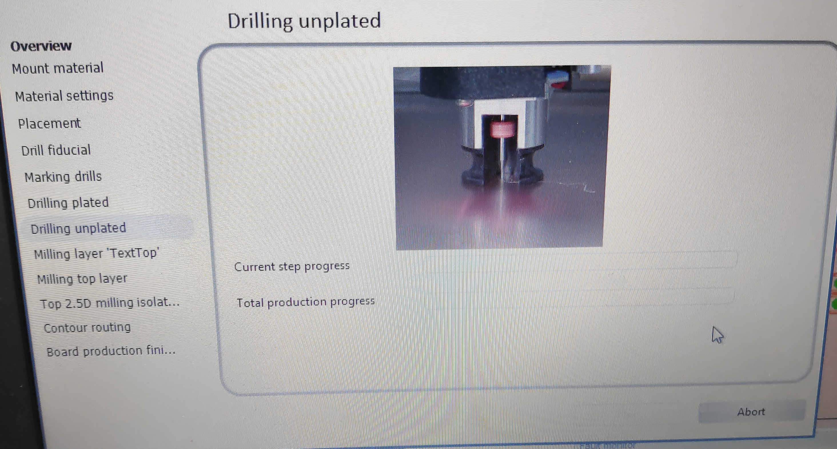
Now open the “board production wizard” and follow the steps. Define the size of the PCB material on the cutting table with the P1 and P2 buttons. Define the PCB material thickness and lace the cutout on the right position. Press start, which will only start the drill job. Afterwards the machine ask for the “milling calibration”, which can be done by placing a line on the PCB material. Make sure that it isn’t place on top of the circuit. If the calibration is, fine press ok and the milling job will start.
The last thing to do with this cutout board is to solder it and test it. To know which components are needed, create a list of each component from the circuit diagram. Prepare all components for the soldering. As stated last weeks, I began with the microcontroller and worked from the inside-out. I followed it up with soldering in the resistors and capacitors. I than added LEDs to the board. Lastly I soldered in the pinheaders, which are soldered from the topside. Here is the list.

With the board assembled it can be tested for short circuits. Check the connection between the GND and VCC with the multimeter, which shouldn’t create a current flow. If a short circuits appears, begin by checking the pinheaders first and flow up by checking the chip and after that each line themselves. When the board is fixed, it can be connected with the programmer board via UPDI. Run a simple program which should turn on the LED on the pin. The power LED should light-up directly, when the board is connected.
Here are the following files used: